电话 : +86-591-86395085
 电子邮件 : sales@uni-optics.com


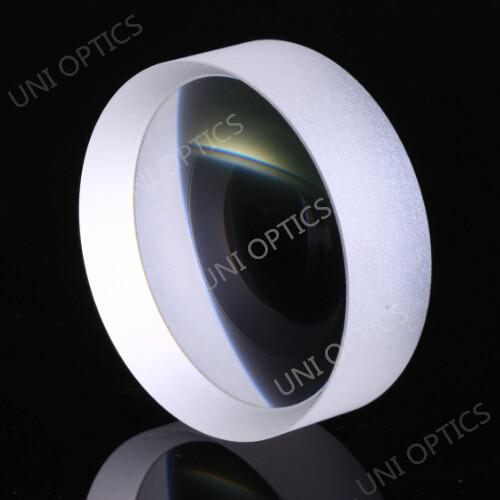
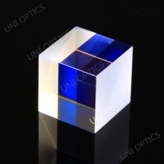
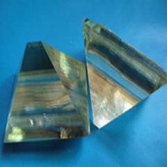
我们的分光板可用于高功率激光系统。在使用分光板时,两个光束在不同的光路中传输,光路取决于入射角和板的厚度。
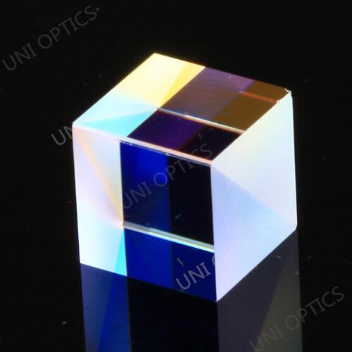
与偏振分光片相比,立体分光棱镜具有以下优势:
*反射光束和透射光束的路径长度相同
*发射光束既不位移也不偏转。
*稳定紧凑
*操作简单
*易于安装/校准
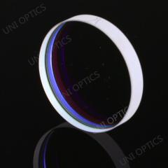
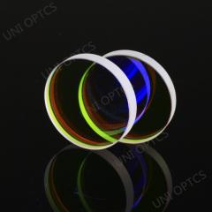
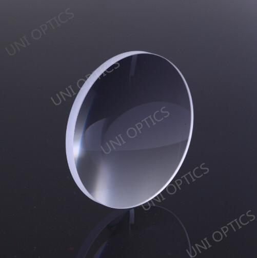
产品规格
材质:N-BK7 A级光学玻璃
尺寸公差:+/-0.1mm
平整度:λ/4@633nm
光束公差:最小3弧分
表面质量:60-40 S/D
通光孔径:>90%
前表面(S1):部分反射镀膜
背面(S2):AR镀膜
斜面:保护
标准镀膜:t/r=50/50±5%,随机偏振;
t=(ts+tp)/2,r=(rs+rp)/2
|
Standard Wavelength(nm) |
Narrow Band | 488, 532, 632.8, 650, 808, 850, 980, 1064, 1310, 1550nm | |||
| Broadband | 450-650, 650-900, 900-1200, 1200-1550, 1500-1610nm | ||||
| Size (mm) | 2.1x2.1x2.1 | 3.2x3.2x3.2 | 5x5x5 | 10x10x10 | |
| 12.7x12.7x12.7 | 20x20x20 | 25.4x25.4x25.4 | 30x30x30 | ||
上一个 :
非偏振分光棱镜(NPBS)下一页 :
可见光和近红外光分光片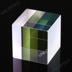 非偏振分光棱镜(NPBS)
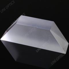
 N-BK7和融石英楔角棱镜
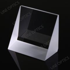
楔角棱镜是一种具有平面倾斜面的光学元件,通常各面以很小的角度相互倾斜,它能将光线转向较厚的部分,通常可以用作隔离元件。楔角棱镜也可以用来产生一个小偏差,不允许光线返回来源。
 红外材料
红外材料
1. Germanium (Ge)
Germanium (Ge) is the preferred lens and window material for high performance infrared imaging systems in the 8–12 μm wavelength band. Its high refractive index makes Ge ideal for low power imaging systems because of minimum surface curvature. Chromatic aberration is small, often eliminating the need for correction.
| Crystallographic properties | |
| Syngony | Cubic |
| Crystal Form | Poly or Single Crystal |
| Lattice Constant | 5.66 |
| Cleavability | <111>, non-perfect |
| Molecular Weight | 72.6 |
| Physical properties | |
| Density, at 20 °C | 5.33 |
| Hardness, Mohs | 6.3 |
| Dielectric Constant for 9.37 × 10⁹ Hz at 300 K | 16.6 |
| Melting | 937 |
| Thermal Conductivity, W/m·K at at 293 K | 59 |
| Thermal Expansion, 1/K at 298 K | 6.1 × 10⁻⁶ |
| Specific Heat Capacity, J/(kgK) at 273-373 K | 0.074 |
| Bandgap, eV | 0.67 |
| Knoop Hardness, kg/mm2 | 800 |
| Youngs Modulus, Gpa | 102.66 |
| Shear Modulus, GPa | 67.04 |
| Bulk Modulus, GPa | 77.86 |
| Debye Temperature, K | 370 |
| Poissons Ratio | 0.278 |
| Elastic Coefficient | C11=129, C12=48.3, C44=67.1 |
| Apparent Elastic Limit | 89.6 MPa (13000psi) |
| Chemical properties | |
| Solubility in water | None |
| Solubility in acids | Soluble |
| Molecular Weight | 72.59 |
2. Silicon (Si)
Silicon (Si) is grown by Czochralski pulling techniques (CZ) and contains some oxygen that causes an absorption band at 9 microns.To avoid this, material can be prepared by a Float-Zone (FZ) process. Optical silicon is generally lightly doped (5 to 40 ohm cm) for best transmission above 10 microns, and doping is usually boron (P-type) and phosphorus (N-type). After doping silicon has a further pass band: 30 to 100 microns which is effective only in very high resistivity uncompensated material.
CZ Silicon is commonly used as substrate material for infrared reflectors and windows in the 1.5-8 micron region. The strong absorption band at 9 microns makes it unsuitable for CO2 laser transmission applications, but it is frequently used for laser mirrors because of its high thermal conductivity and low density. Application as window, lens in the 1.5 - 8 um region; Mirror for CO2 laser and spectrometer applications.
Crystallographic properties
Syngony
Cubic
Lattice Constant, A
5.43
Physical properties
Density
2.33g/cm3
Hardness, Mohs
7
Dielectric Constant for 9.37 x 10⁹ Hz
13
Melting point, оС
1414
Thermal Conductivity, W/m·K at 313 K
163
Thermal Expansion, 1/K at 293 K
2.6x10⁻⁶
Specific Heat Capacity, J/(kg°C)
712.8
Bandgap, eV
1.1
Knoop Hardness, kg/mm2
1100
Youngs Modulus, Gpa
130.91
Shear Modulus, GPan
79.92
Bulk Modulus, GPa
101.97
Debye Temperature, K
640
Poissons Ratio
0.28
Chemical properties
Solubility in water
None
Molecular Weight
28.09
3、ZnS material:
ZnS MultiSpectral Under intense heat and pressure, defects within the crystalline lattice are virtually eliminated, leaving a water-clear material with minimal scatter and high transmission characteristics from 0.4 to 12 microns. This material is particularly well suited for high-performance common aperture systems that must perform across a broad wavelength spectrum.
Specifications:
Material: ZnS MultiSpectral
Diameter Tolerance: --------------------- +0.0, -0.1mm
Thickness Tolerance: -------------------- ±0.1mm
Clear Aperture: ---------------------------->85%
Parallelism: -----------------------------------3 arc minute
Surface Quality: ----------------------------80-50 scratch and dig
Wavefront Distortion: -------------------- λ /2 per 25mm @633mm
Bevel: -----------------------------------------Protective (<0.2mm x 45° )
Coating: -------------------------------------- Optional (Uncoated, AR Coating, etc.)
4. ZnSe material
ZnSe is a preferred material for lenses, windows, output couplers and beam expanders for its low absorptivity at infrared wavelengths and its visible transmission. For high-power applications, it’s critical that the material bulk absorption and internal defect structure be carefully controlled, that minimum-damage polishing technology be employed, and the highest quality optical thin-film coatings are used. The material absorption is verified by CO2 laser vacuum calorimetry. Our quality assurance department provides testing and specific optics certification on request.
ZnSe is non-hygroscopic and chemically stable, unless treated with strong acids. It’s safe to use in most industrial field, and laboratory environments.
 激光晶体
激光晶体
晶体最适用于激光应用。 UNI OPTICS提供以下晶体产品。
1.激光晶体和棒:YAG晶体,Nd:YVO4晶体
2.非线性晶体:BBO,KTP,LiNbO3,LBO。KDP&DKDP
3.双折射晶体:YVO4,a-BBO,方解石。
 BK7和熔融石英玻璃道威棱镜
道威棱镜由H.W.多芬发明,多芬棱镜也被称为反转棱镜。当棱镜绕其长轴旋转时,通过棱镜所看到的图像的旋转速度是棱镜旋转速度的两倍。道威棱镜比较特殊,有时用于特殊的应用。入口和出口表面都有防反射涂层
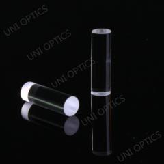 棒透镜
棒透镜
用于光纤耦合和激光二极管光束成形,工作距离为0mm的透镜非常适用于单模和多模光纤和激光二极管的准直,因为透镜可以直接定位并直接粘合在发射源上。 对于聚焦应用,或者镜头不能与发射源直接接触的情况下,所有镜头也可以具有小的工作距离。UNI Optics可提供Φ1~Φ15mm的尺寸,数量和尺寸,包括抛光/磨削表面的差异,可根据客户要求提供。